Полная версия:
Все науки. №10, 2024. Международный научный журнал
Рис. 16. Третье представление потенциальной картины кристаллического кремния в масштабе 10—2 и 10—3 единицы x, y
Рис. 17. Второе представление потенциальной картины кристаллического кремния в масштабе 10—5 и 10—6 единицы x, y
Рис. 18. Второе представление потенциальной картины кристаллического кремния в масштабе 10—5 и 10—6 единицы x, y
Рис. 19. Второе представление потенциальной картины кристаллического кремния в масштабе 10—5 и 10—6 единицы x, y
В результате смоделированных трёхмерных графиков можно наглядно проследить, что каждый из графиков гладкий и простейший, в отличие от предыдущих двух примеров, где участвовали легированные соединения теллурида кадмия и оксида кремния. В данном случае смоделирован кристаллический чистый кремний, что позволяет получать указанные графики, коррелирующие с действительностью.
Выводы
Исходя из полученных результатов, были сформулированы 3 отдельно взятые модели по теллуриду кадмия, оксиду кремния и кристаллическому кремнию, при этом в каждом из случаев функции представлены в трёхмерном пространстве. Фактически, было бы логичным расположить каждую из функций друг за другом, создав одну единую модель полупроводникового элемента.
Так, в виде максимально дискретно представленного графика, моделирующий весь полупроводниковый элемент может быть представлен сборник всех на данный момент полученных трёхмерных графиков в различных комбинациях, что также соответствует различным комбинациям расположения слоёв полупроводникового элемента. При этом каждая из комбинаций может быть представлена посредством отдельных выборок, где отдельная роль отводиться 2 измерениям, а третья изменяется, соответствуя общей выборке в Табл. 2—4.
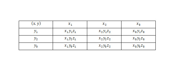
Таблица 1. Первая формулировка комплектов графиков
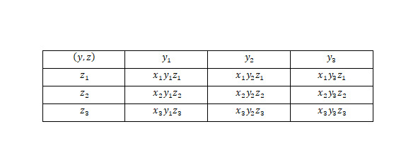
Таблица 2. Вторая формулировка комплектов графиков
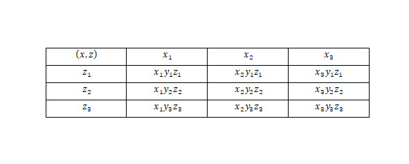
Таблица 3. Вторая формулировка комплектов графиков
При этом каждая таблица может быть представлена в 2 масштабах 10—2, 10—3 в Рис. 20—22, при том же равная по виду с масштабов по 10—5 и 10—6.
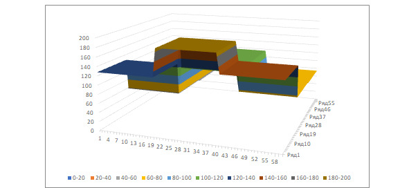
Рис. 20. Первая форма соединённой трёхмерной диаграммы в 10—2 и 10—3
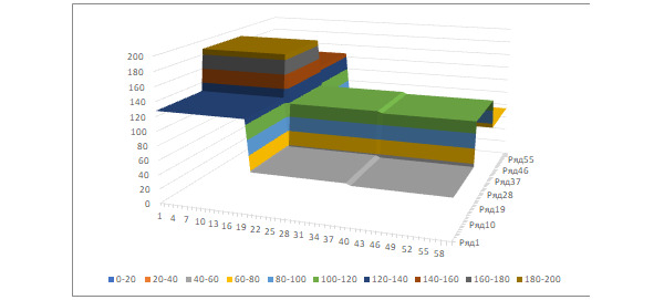
Рис. 21. Вторая форма соединённой трёхмерной диаграммы в 10—2 и 10—3
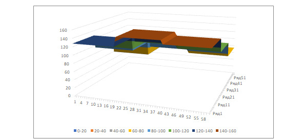
Рис. 22. Третья форма соединённой трёхмерной диаграммы в 10—2 и 10—3
В результате была получена дискретная общая форма организованного полупроводникового элемента, однако при организованном эмпирическом расчёте полученная вариация может быть представлена согласно детектируемым показателям. Так, зависимости спектрального характера при взаимодействии с внешним коронным разрядом показывают изменение Рис. 24, когда же изменение высоты в масштабе потенциального барьера, необходимого для преодоления электронами могут быть представлены согласно Рис. 23.
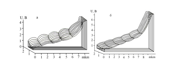
Рис. 23. Рост потенциального барьера электронов с наличие стороннего источника потенциального поля
Рис. 24. Спектральный характер взаимодействия под действием стороннего электростатического поля
Каждый из полученных результатов на данный момент является важным и актуальным элементом исследования, который наглядно подтверждается согласно степени корреляции с полученными теоретическими данными в рамках постановки граничных условий для выведенного уравнения электропроводности.
Заключение
В результате исследования был представлен алгоритм моделирования, позволяющий описать явления класса электропроводности, под действием стороннего поля. В том числе большое внимание было уделено непосредственной стадии моделирования в статичной форме полупроводниковому элементу типа n-p-n, состоящий из теллурида кадмия, оксида кремния и кристаллического кремния. Дальнейшие работы в настоящем направлении являются также актуальными, наряду с последующим сведением в аналитический вид комплексной сборки элементов и их комбинаций, участвующие в сборке исследованного в настоящей работе полупроводникового элемента.
Использованная литература
1. Deng, Z., Li, K., Priimagi, A. et al. Light-steerable locomotion using zero-elastic-energy modes. Nat. Mater. (2024). https://doi.org/10.1038/s41563-024-02026-4
2. Lee, KJ., Cros, V. & Lee, HW. Electric-field-induced orbital angular momentum in metals. Nat. Mater. 23, 1302—1304 (2024). https://doi.org/10.1038/s41563-024-01978-x
3. Lin, X., Zhang, S., Yang, M. et al. A family of dual-anion-based sodium superionic conductors for all-solid-state sodium-ion batteries. Nat. Mater. (2024). https://doi.org/10.1038/s41563-024-02011-x
4. An approach to identify and synthesize memristive III—V semiconductors. Nat. Mater. 23, 1322—1323 (2024). https://doi.org/10.1038/s41563-024-01991-0
5. Liu, L., Ji, Y., Bianchi, M. et al. A metastable pentagonal 2D material synthesized by symmetry-driven epitaxy. Nat. Mater. 23, 1339—1346 (2024). https://doi.org/10.1038/s41563-024-01987-w
6. Li, Z., Zhai, L., Zhang, Q. et al. 1T′-transition metal dichalcogenide monolayers stabilized on 4H-Au nanowires for ultrasensitive SERS detection. Nat. Mater. 23, 1355—1362 (2024). https://doi.org/10.1038/s41563-024-01860-w
7. Miura, M., Eley, S., Iida, K. et al. Quadrupling the depairing current density in the iron-based superconductor SmFeAsO1—xHx. Nat. Mater. 23, 1370—1378 (2024). https://doi.org/10.1038/s41563-024-01952-7
8. Hackett, L., Koppa, M., Smith, B. et al. Giant electron-mediated phononic nonlinearity in semiconductor—piezoelectric heterostructures. Nat. Mater. 23, 1386—1393 (2024). https://doi.org/10.1038/s41563-024-01882-4
9. Bae, J., Won, J., Kim, T. et al. Cation-eutaxy-enabled III—V-derived van der Waals crystals as memristive semiconductors. Nat. Mater. 23, 1402—1410 (2024). https://doi.org/10.1038/s41563-024-01986-x
10.Wang, X., Pan, C., Xia, N. et al. Fracture-driven power amplification in a hydrogel launcher. Nat. Mater. 23, 1428—1435 (2024). https://doi.org/10.1038/s41563-024-01955-4
11.Figgener, J., van Ouwerkerk, J., Haberschusz, D. et al. Multi-year field measurements of home storage systems and their use in capacity estimation. Nat Energy (2024). https://doi.org/10.1038/s41560-024-01620-9
12.Tregnago, G. Combining photovoltaic elements. Nat Energy 9, 1052 (2024). https://doi.org/10.1038/s41560-024-01647-y
13.Flexible participation of electrosynthesis in dynamic electricity markets. Nat Energy 9, 1062—1063 (2024). https://doi.org/10.1038/s41560-024-01584-w
14.Choo, S., Lee, J., Şişik, B. et al. Geometric design of Cu2Se-based thermoelectric materials for enhancing power generation. Nat Energy 9, 1105—1116 (2024). https://doi.org/10.1038/s41560-024-01589-5
15.Wang, J., Chortos, A. Performance metrics for shape-morphing devices. Nat Rev Mater 9, 738—751 (2024). https://doi.org/10.1038/s41578-024-00714-w
16.Shan, H., Poredoš, P., Chen, Z. et al. Hygroscopic salt-embedded composite materials for sorption-based atmospheric water harvesting. Nat Rev Mater 9, 699—721 (2024). https://doi.org/10.1038/s41578-024-00721-x
17.Parvesh Chander, Alisha Arora, Ankita Singh, Mohit Madaan, Nagendra Prasad Pathak, V.K. Malik. Exploration of room temperature magnetodielectric behavior in Nd0.5Dy0.5FeO3 thin films and transmission line resonators in GHz frequency range. Physica B: Condensed Matter. Volume 694, 1 December 2024, 416431 https://doi.org/10.1016/j.physb.2024.416431
18.Naqash Hussain Malik, Shafaat Hussain Mirza, Sikander Azam, Muhammad Farooq Nasir, Muhammad Jawad, Nargis Bano, Muhammad Zulfiqar. Exploring the impact of hydrostatic pressure on the essential physical properties of BaTiO3 perovskite: A first principles quantum investigation and prospects for optoelectronic and thermoelectric applications. Physica B: Condensed Matter. Volume 694, 1 December 2024, 416430. https://doi.org/10.1016/j.physb.2024.416430
19.Dung Dang Duc, Luong Thi Kim Phuong, Nguyen Huu Lam, Duong Van Thiet, Luong Hong Dang, Nguyen Hoang Thoan, Vu Tien Lam, Duong Quoc Van. Optical, magnetic and electrical properties of new binary MnTiO3-modified Ba (Zr, Ti) O3 materials as solid solution. Physica B: Condensed Matter. Volume 694, 1 December 2024, 416444 https://doi.org/10.1016/j.physb.2024.416444
20.S. Asadi Toularoud, H. Hadipour, H. Rahimpour Soleimani. Engineering the electronic and magnetic properties of monolayer TiS2 through systematic transition-metal doping. Physica B: Condensed Matter. Volume 694, 1 December 2024, 416413.
https://doi.org/10.1016/j.physb.2024.416413
21.Wael M. Mohammed, M.M. El-Desoky, N. Abdllah, Hamdy F.M. Mohamed, E.E. Abdel-Hady, D.E. El Refaay. Relationship between structural, electrical properties and positron annihilation parameters of V2O5—Cu2O—P2O5 glasses. Physica B: Condensed Matter. Volume 694, 1 December 2024, 416459. https://doi.org/10.1016/j.physb.2024.416459
22.Qihong Wen, Yifu Li, Baoqiang Xu, Hongwei Yang. Prediction of azeotropic behavior using physicochemical properties for Sn-based binary liquid alloys in vacuum distillation. Physica B: Condensed Matter. Volume 694, 1 December 2024, 416415.
https://doi.org/10.1016/j.physb.2024.416415
MODULAR APPARATUS FOR NUCLEAR REACTIONS SPECTROSCOPY (MARS)
UDK: 538.56/.569.4
L. Garrido-Gómeza,∗, M. A. G. Alvareza, J. P. Fernández-Garcíaa, A. Vegas-Díaza, b, B. Fernándeza, b, F. J. Ferrera, b, D. Lopez-Airesc
aDepartamento FAMN, Universidad de Sevilla, Apartado 1065, 41080, Sevilla, Spain, bCentro Nacional de Aceleradores, Universidad de Sevilla, Junta de Andalucía-CSIC, 41092, Sevilla, Spain, cEuropean Commission- Joint Research Centre, Institute for Transuranium Elements ITU, Box 2340, 76125, Karlsruhe, Germany
Abstract. MARS (Modular Apparatus for nuclear Reactions Spectroscopy) consists of a compact, portable and, therefore, versatile spectrometer for measuring nuclear reactions and carrying out energy spectroscopy. MARS, as a system, is com posed by 3 sub-systems: detection, electronic, and data acquisition. The de tection sub-system is based on 16 silicon (Si) SBD (Surface Barrier Detectors) from ORTEC, being 8 detectors 15 µm thick and 8 detectors 500 µm thick (nominal values). Thus, MARS allows for coupling 8 Si telescopes. Detectors are connected to an electronic system based exclusively on desktop and VME modules from CAEN (Costruzioni Apparecchiature Elettroniche Nucleari) SpA company. A PC handles the data acquisition by means of CoMPASS (CAEN Multi-PArameter Spectroscopy Software). It manages parameters, builds plots, and saves the relevant energy and time spectra. MARS has been developed in collaboration with CAEN SpA (electronics developer and manufacturer) and ATI Sistemas SL (CAEN SpA commercial representative in Spain). The multi channel feature of MARS allows for measuring angular and energy distributions of charged particles outgoing from a nuclear reaction. This work aims to present MARS as a spectrometer and its characterization. It includes a measurement of the 6Li+12C nuclear reaction, carried out at the 3MV tandem of the CNA (National Accelerator Centre), in Seville, Spain.
Keywords: Nuclear instrumentation, Spectrometer, Digitizers, Silicon detectors, 6Li +12C, Transfer reactions
Introduction
In the XXIcentury radiation detection and measurement evolution is strongly linked to two main features: i) the increasing use of digital techniques in process ing pulses from detectors and ii) the increasing trend of digitizing pulses closer to radiation detectors. As a consequence, the basic components in a typical pulse processing electronic chain are in continuous development [1, 2].
An incident radiation quantum interacts within the detector and deposits energy, that commonly produces free charges and a consequent current pulse. The integrated charge tends to be proportional to the energy deposited by the incident quantum. The preamplifier, commonly with a charge sensitive config uration, converts the current pulse into a voltage one, whose height is propor tional to the integrated charge. The preamplifier is also responsible for coupling impedance and constitutes an interface between the detector and the processing electronic. Recording the pulse height distribution is the basis to study the energy distribution of the incident radiation, allowing for energy spectroscopy [1, 2]. Traditional digital technologies, for instance, 8—10 bits ADCs (Analog-to Digital Converters), benefit from shaping amplifiers, that convert the pream plifier output voltage pulse into an ideally Gaussian shape, suitable for mea surements, in between preamplification and digitalization processes [1]. New digital technologies (for instance, 12—16 bits digitizers) [3, 4, 5, 6, 7, 8, 9] al low for pulse processing directly from the preamplifier (or even from detector, depending on the detector and the application), sampling a preamplified pulse with high digital resolution. The preamplifiers are characterized by a shaping time constant related to the duration of the pulse at its output. Shaped pulses are commonly sent to circuits that select them for further processing. For instance, an integral discriminator selects pulse height (and therefore energy) above a certain threshold; a differen tial discriminator or SCA (Single Channel Analyzer), selects pulse amplitudes between an upper and a lower threshold [1, 2]. The MCA (Multi Channel An alyzer) measures the pulse height for each selected event, assigning the pulse height to one of the acquisition bins or channels. It increments a memory register for the appropriate bin/channel. The final statistical result is a histogram con taining the number of pulses (events) within each of its amplitude (bin/channel). The resulting histogram or pulse height spectrum consists of digital values that can be displayed and stored for further processing and analysis. Pulse height spectrum represents the main tool for carrying out spectroscopy [2]. There have been 3 major data acquisition standards used in nuclear and par ticle Physics. NIM (Nuclear Instrumentation Module) is used to power supply the electronics [1, 10]. NIM modules cannot communicate through the crate backplane. This is a feature of later standards CAMAC and VME. As a conse quence, NIM-based ADC modules are nowadays uncommon. NIM is still widely used for amplifiers, discriminators, and other logic modules that do not require digital data communication [1]. CAMAC (Computer-Aided Measurement And Control) went further and consists of a standard bus and modular-crate elec tronics for data acquisition and control. The bus allows data transfer, through the crate backplane, between plug-in modules and a crate controller interfaces to a PC. The current standard is VME (VERSA Module Eurocard), expanded from CAMAC by providing more options and a faster bus speed [1]. VME bus was originally developed as a computer bus and has since been adapted for its use in nuclear and particle physics applications.
Each module is a printed circuit board (PCB) that connects to the backplane with pin sets. The backplane supplies the modules with DC voltage of +/-5 V and +/-12 V. Associated pins connect between modules to create a bus. VMEbusmodulescommunicatethroughdigital signals bussed over the back plane and data transfer occurs by direct memory access. Analog input and output may occur through the front panel using LEMO 00, ribbon, or MCX connectors. VME bus modules offer the same utility as NIM and CAMAC ones, including power supplies, discriminators, and amplifiers; however, parameters are often set through software control, allowing automated and/or remote con trol of parameters. The GUI (Graphical User Interface) software may reside on an embedded computer within a VME bus module. Interfacing with PCs occurs by means of USB, PCI, or other connections. VME bus can be extended to multicrate systems through bridge cards. Other protocols such as Ethernet connections can be used to link sub-racks into a common network or with a single PC. Overcoming the limitations and limits of traditional analog acquisition chains, new waveform digitizers have been developed [5, 6, 7, 8, 9]. They consist in many models differing in sampling frequency, resolution, number of channels, form factor, and memory size among others. In parallel with hardware development, different efforts were dedicated to developing DPP (Digital Pulse Processing) algorithms [11, 12, 13, 14]. A DPP algorithm can be installed in an FPGA (Field Programmable Gate Array) of the digitizer allowing online analysis and implementing new acquisition methods that go beyond the simple waveform record. Regarding to the waveform digitizers, the basic principle is to acquire the complete pulse, convert it to digital, by using a fast ADC, and then perform calculations on the digital data directly on an FPGA available on board. A dig itizer with DPP becomes thus a new instrument that represents a fully digital replacement of most traditional modules such as discriminators, S/MCA, QDC (Charge (Q) to Digital Converter), TDC (Time to Digital Converter), among others. Digitizers are available in different form factors (VME, NIM, and desk top) and represent the state-of-the-art result of all experiences collected in pulse processing and data acquisition systems.
MARS description
MARS (Modular Apparatus for nuclear Reactions Spectroscopy) is composed of detection, electronic, and acquisition systems. MARS electronics combine desktop and VME form factors. It is a portable and versatile spectrometer for measuring angular and energy distributions of charged particles outgoing nuclear reactions. Its modular and advanced design allows components to be exchanged (e.g. change detectors to measure different types of radiation), besides applying different types of digitizers, firmware, and then acquisition systems. In par ticular, the application of different firmware allows for different pulse analysis techniques.
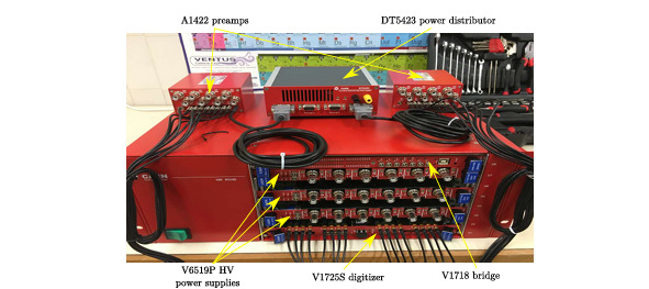
Figure 1: MARS electronic system. It is based exclusively on desktop and VME form factors from CAEN SpA.
2.1. MARS detection system
The detection system is composed of 16 semiconductor planar totally de plected silicon (Si) SBD (Surface Barrier Detectors) from ORTEC with active areas of 50 mm2. Eight of them have 15 µm thickness (model ED-35-050-15), and the other eight have 500 µm thickness (model TB-15-050-500) (nominal values). These detectors are suitable for the identification of charged particles and their respective high-resolution spectroscopy. The manufacturer specifies a resolution of 15 keV for 241Am alphas (5.486 MeV (corresponding to 85% of intensity)) [15, 16].
2.2. MARS electronic system
Figure 1 presents MARS electronic system. It is based on desktop and VME modules from CAEN SpA:
– TwoA1422 charge sensitive preamplifiers. They present a sensitivity of 90 mV/MeV (for Si detectors) and support a detector capacitance up to 200 pF (F2 type). The A1422 are implemented into alloy boxes, 8 channels each, and feature BNC connectors for the input (detector), SHV for high voltage supply, LEMO for the energy output and the input test (TEST IN), and a cable with a D – type 9 pin male connector for the power supply [17].
– The DT5423 power distributor provides 4 standard D-type 9 pin fe male connectors to supply up to 4 A1422 preamplifiers with ± 12 V [18].
An alternative VME form factor module [19] could be employed and inte grated in the same VME crate described below.
– Three V6519P HV power supply modules provide the high voltage (up to 500 V and 3 mA of voltage and current, respectively) to the de tectors. Each one houses 6 HV power supply channels that are controlled by software. The channels share a common floating return which allows on-detector grounding, reducing the noise level. HV outputs are delivered by SHV connectors [20].– The V1725S digitizer consists of 16 (0—15) input channels capable of recording waveforms (directly from the preamplifiers A1422 [17]) along with performing advanced algorithms for online DPP [21]. Using DPP f irmware, we are able to acquire the integrated charge and carry out PSD (Pulse Shape Discrimination) and PHA (Pulse Height Analysis), as well as read out waveforms with automatic pulse identification. It features 14 bit resolution, 250 MS/s sampling rate, and 2 V input range. This implies a digital precision of 0.12 mV and a digital resolution of 0.006%, with a processing time of 65 µs. Communication with the board can be done through the VME bus and Optical Link. It is well suited for mid fast pulses such as the ones coming from silicon detectors coupled to the charge sensitive preamplifiers A1422 [17].
– The V1718 bridge is a VMEtoUSB2.0 bridge. It acts as a VME master module and can be operated from a USB port of a standard PC [22].
– The VME8008Bisan8slotVME cratesuitable for 6U x 160 mmboards, which serves as a support and power supply for the electronic modules V6519P, V1725S, and V1718 [23].
2.3. MARS acquisition system
The V1725S digitizer runs the DPP-PSD/PHA firmware. The digitizer im plements a digital replacement of discriminator, pulse shaping, and gate gener ator. These functions are performed inside the FPGA (onboard) without using external cables, delay lines and/or other boards. The V1725S digitizer itself con sists of a multi-channel data acquisition system that replaces traditional analog boards and constitutes a single compact tool for nuclear reactions spectroscopy. A PC with an Intel i7 (1.8 GHz, 8 CPUs) and 16 GB RAM handles the data acquisition by means of CoMPASS (CAEN Multi-PArameter Spectroscopy Software) [24]. CoMPASS represents the GUI, manages parameters, builds plots and saves the energy and time spectra. Within CoMPASS, we can set discriminator parameters such as: threshold, discrimination type, and trigger holdoff. In addition, we can set parameters related to PHA: trapezoid rise time, flat top, pole-zero; parameters related to PSD: pre-gate, short gate and long gate; as well as the gain and the number of channels of the spectra. It also allows to discard pile-up and saturation events besides applying energy, time, and PSD filters.
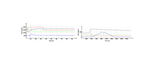
(a) PSD firmware. The input signal (black) within the long and short gates (red and green squared pulses). At the bottom, we have the constant fraction discriminator (CFD) signal (blue). (b) PHA firmware. The input signal (black with long tail), the fast trigger (left red), and the trapezoid filter (blue) with the peaking signal (green) just below the trapezoid. Figure 2: CoMPASS screenshots showing different electronic signals for (a) PSD firmware, and (b) PHA firmware.
Moreover, the V1725S digitizer has a logic unit that allows for measuring coincidences. Through CoMPASS, we are able to acquire events in logic AND between pairs of consecutive data acquisition chains (ch0 & ch1 || ch2 & ch3 || and so on). For this, a coincidence (time) window must be enabled and defined. Once the first detector is triggered, any signal triggering the second detector, within the specified time window, will validate an event (in coincidence). Anti coincidences can also be performed using external logic modules and using the generated gate as an input to the digitizer trigger input.